About VLSI..
Monday, December 17, 2012
Graphic Data System II
standard for data exchange of integrated circuit or IC layout artwork.
It is a binary file format representing planar geometric shapes, text
labels, and other information about the layout in hierarchical form.
The data can be used to reconstruct all or part of the artwork to be
used in sharing layouts, transferring artwork between different tools,
or creating photo masks. Initially, GDS II was designed as a format
used to control integrated circuit photo mask plotting. Despite its
limited set of features and low data density, it became the industry
conventional format for transfer of IC layout data between design
tools of different vendors, all of which operated with proprietary
data formats. It was originally developed by Calma for its layout
design software, "Graphic Data System" ("GDS") and "GDS II". Now the
format is owned by Cadence Design Systems.
GDS II files are usually the final output product of the IC design
cycle and are given to IC foundries for IC fabrication. GDS II files
were originally placed on magnetic tapes. This moment was fittingly
called tape out though it is not the original root of the term.
Objects contained in a GDS II file are grouped by assigning numeric
attributes to them including "layer number", "datatype" or "texttype".
While these attributes were designed to correspond to the "layers of
material" used in manufacturing an integrated circuit, their meaning
rapidly became more abstract to reflect the way that the physical
layout is designed. As of October 2004, many EDA software vendors have
begun to support a new format, OASIS, which may replace GDS I
source:http://www.layouteditor.net/wiki/GDSII
Thursday, May 3, 2012
VEDA IIT Recruitment Test - 26th May 2012
'VEDA IIT Recruitment Test' is scheduled on 26th May 2012 . Apply online at www.vedaiit.com before 23rd May 2012
VEDA IIT Recruitment Test Details:
Exam Date : *Entrance Test will be conducted on 26th May 2012
Exam Time : 10:00 A.M
Exam Duration : 3 Hours
Last Date to Apply: DD for Rs.300/- should be drawn in favor of VEDA Institute of Information Technology Pvt. Ltd., Hyderabad should reach VEDA IIT by 23rd May 2012
How to Apply : Please visit www.vedaiit.com and click on 'Apply for Jobs'
Venue : VEDA IIT, Plot No. 90,
Annapurna Studios/ VEDA Lane,
Road No 2, Banjara Hills,
Hyderabad
Phone: + 91 40 3061 5555
or
JNTUH ,hyderabad kukatpalli.
Syllabus : 1. Digital Design & Micro Processors
2. C Programming
3. Aptitude
Saturday, March 3, 2012
Recruitment of Engineer Trainees in VLSI Design (Logic/Physical) and Embedded System Design at VEDAIIT for March 2012
Monday, January 23, 2012
VLSI Terminology: Definition of process technology
With regard to digital integrated circuits, process technology refers to the particular method used to make silicon chips. The driving force behind the manufacture of integrated circuits is miniaturization, and process technology boils down to the size of the finished transistor and other components. The smaller the transistors, the more transistors in the same area, the faster they switch, the less energy they require and the cooler the chip runs (given equal numbers of transistors).
Measured in Nanometers
The size of the features (the elements that make up the structures on a chip) used to be measured in micrometers. A 3 µm process technology, also called a "technology node" and "process node," referred to a silicon chip with features three micrometers in size. Today, features are measured in nanometers. A 45 nm process technology refers to features 45 nm or 0.45 µm in size.
Elements Measured
Historically, the process technology referred to the length of the silicon channel between the source and drain terminals in field effect transistors (see FET). The sizes of other features are generally derived as a ratio of the channel length, where some may be larger than the channel size and some smaller. For example, in a 90 nm process, the length of the channel may be 90 nm, but the width of the gate terminal may be only 50 nm.
An Example of Progress
Consider that the process technology of the first 486 chip in 1989 was one micron (1,000 nanometers). By 2003, the state-of-the-art decreased to 90 nm ("90 nano"). In 15 years, feature sizes were reduced by slightly less than one millionth of a meter. What may seem like a minuscule, microscopic change to the casual observer took thousands of man years and billions of dollars worth of research and development. Note the huge variance in semiconductor feature sizes starting in the 1950s (see chart below).
Chips Are Nanotechnology
Intel introduced 45 nm processors in 2008. To understand how tiny 45 nanometers is, it would take two thousand 45 nm objects laid side-by-side to equal the thickness of one human hair.
In 2010, 32 nm chips were introduced, and feature sizes as low as 11 nm are expected in the future. For some time, chips have been in the realm of nanotechnology, which refers to elements 100 nanometers and smaller.
Definition of: feature size
Integrated circuits: Generations
SSI, MSI and LSI
The first integrated circuits contained only a few transistors. Called "small-scale integration" (SSI), digital circuits containing transistors numbering in the tens provided a few logic gates for example, while early linear ICs such as the Plessey SL201 or the Philips TAA320 had as few as two transistors. The term Large Scale Integration was first used by IBM scientist Rolf Landauer when describing the theoretical concept[citation needed], from there came the terms for SSI, MSI, VLSI, and ULSI.
VLSI
Sunday, January 8, 2012
AWK :The for statement
The for Statement
The for statement makes it more convenient to count iterations of a loop. The general form of the for statement looks like this:
for (initialization; condition; increment) body
This statement starts by executing initialization. Then, as long as condition is true, it repeatedly executes body and then increment. Typically initialization sets a variable to either zero or one, increment adds 1 to it, and condition compares it against the desired number of iterations.
Here is an example of a for statement:
awk '{ for (i = 1; i <= 3; i++) print $i }' This prints the first three fields of each input record, one field per line.
In the for statement, body stands for any statement, but initialization, condition and increment are just expressions. You cannot set more than one variable in the initialization part unless you use a multiple assignment statement such as x = y = 0, which is possible only if all the initial values are equal. (But you can initialize additional variables by writing their assignments as separate statements preceding the forloop.)
awk '{ for (i =j= 1; i <= 3; i++)
{if (j <2){
j++;
print $i
}
}'
The same is true of the increment part; to increment additional variables, you must write separate statements at the end of the loop. The C compound expression, using C's comma operator, would be useful in this context, but it is not supported in awk.
Most often, increment is an increment expression, as in the example above. But this is not required; it can be any expression whatever. For example, this statement prints all the powers of 2 between 1 and 100:
for (i = 1; i <= 100; i *= 2) print i
Any of the three expressions in the parentheses following the for may be omitted if there is nothing to be done there. Thus, `for (;x > 0;)' is equivalent to `while (x > 0)'. If the condition is omitted, it is treated as true, effectively yielding an infinite loop (i.e., a loop that will never terminate).
In most cases, a for loop is an abbreviation for a while loop, as shown here:
initialization while (condition) { body increment }source:http://www.staff.science.uu.nl/~oostr102/docs/nawk/nawk_toc.html#TOC77
Monday, January 2, 2012
Definition of Metastability...
source: | ||
 | Definition of Metastability : | |
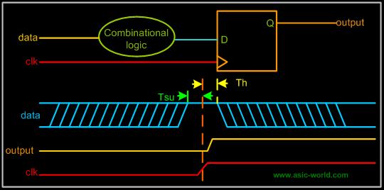
Whenever there are setup and hold time violations in any flip-flop, it enters a state where its output is unpredictable: this state is known as metastable state (quasi stable state); at the end of metastable state, the flip-flop settles down to either '1' or '0'. This whole process is known as metastability. In the figure below Tsu is the setup time and Th is the hold time. Whenever the input signal D does not meet the Tsu and Th of the given D flip-flop, metastability occurs. | ||
| ||
 | ||
| ||
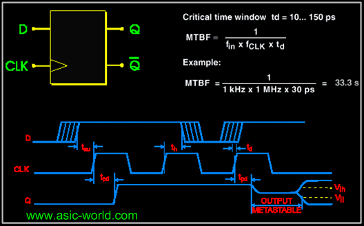
When a flip-flop is in metastable state, its output oscillate between '0' and '1' as shown in the figure below (here the flip-flop output settles down to '0') . How long it takes to settle down, depends on the technology of the flip-flop. | ||
| ||
|
| ||
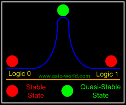
| | If we look deep inside of the flip-flop we see that the quasi-stable state is reached when the flip-flop setup and hold times are violated. Assuming the use of a positive edge triggered "D" type flip-flop, when the rising edge of the flip-flop clock occurs at a point in time when the D input to the flip-flop is causing its master latch to transition, the flip-flop is highly likely to end up in a quasi-stable state. This rising clock causes the master latch to try to capture its current value while the slave latch is opened allowing the Q output to follow the "latched" value of the master. The most perfectly "caught" quasi-stable state (on the very top of the hill) results in the longest time required for the flip-flop to resolve itself to one of the stable states. | |
| ||
 | ||
| ||
 | How long does it stay in this state? | |
The relative stability of states shown in the figure above shows that the logic 0 and logic 1 states (being at the base of the hill) are much more stable than the somewhat stable state at the top of the hill. In theory, a flip-flop in this quasi-stable hilltop state could remain there indefinitely but in reality it won't. Just as the slightest air current would eventually cause a ball on the illustrated hill to roll down one side or the other, thermal and induced noise will jostle the state of the flip-flop causing it to move from the quasi-stable state into either the logic 0 or logic 1 state. | ||
| ||
| ||
 | What are the cases in which metastability occurs? | |
| As we have seen that whenever setup and hold violation time occurs, metastability occurs, so we have to see when signals violate this timing requirement: | ||
| ||
| ||
| ||
 | What is MTBF? | |
MTBF is Mean time between failure, what does that mean? Well MTBF gives us information on how often a particular element will fail or in other words, it gives the average time interval between two successive failures. The figure below shows a typical MTBF of a flip-flop and also it gives the MTBF equation. I am not looking here to derive MTBF equation :-) | ||
| ||
 | ||
| | ||
| | ||
| | ||
| | ||
| | ||
| | ||
| | ||
Normally, | ||
|
| ||
| |
| |
| ||
 | METASTABILITY REFERENCES | |
| ||
|
Setup and hold times of an flip-flop
Setup and hold times
Setup time is the minimum amount of time the data signal should be held steady before the clock event so that the data are reliably sampled by the clock. This applies to synchronous circuits such as the flip-flop.
Hold time is the minimum amount of time the data signal should be held steady after the clock event so that the data are reliably sampled. This applies to synchronous circuits such as the flip-flop.
To summarize: Setup time -> Clock flank -> Hold time.
The metastability in flip-flops can be avoided by ensuring that the data and control inputs are held valid and constant for specified periods before and after the clock pulse, called the setup time (tsu) and the hold time (th) respectively. These times are specified in the data sheet for the device, and are typically between a few nanoseconds and a few hundred picoseconds for modern devices.
Unfortunately, it is not always possible to meet the setup and hold criteria, because the flip-flop may be connected to a real-time signal that could change at any time, outside the control of the designer. In this case, the best the designer can do is to reduce the probability of error to a certain level, depending on the required reliability of the circuit. One technique for suppressing metastability is to connect two or more flip-flops in a chain, so that the output of each one feeds the data input of the next, and all devices share a common clock. With this method, the probability of a metastable event can be reduced to a negligible value, but never to zero. The probability of metastability gets closer and closer to zero as the number of flip-flops connected in series is increased.
So-called metastable-hardened flip-flops are available, which work by reducing the setup and hold times as much as possible, but even these cannot eliminate the problem entirely. This is because metastability is more than simply a matter of circuit design. When the transitions in the clock and the data are close together in time, the flip-flop is forced to decide which event happened first. However fast we make the device, there is always the possibility that the input events will be so close together that it cannot detect which one happened first. It is therefore logically impossible to build a perfectly metastable-proof flip-flop.
Propagation delay
Another important timing value for a flip-flop (F/F) is the clock-to-output delay (common symbol in data sheets: tCO) or propagation delay (tP), which is the time the flip-flop takes to change its output after the clock edge. The time for a high-to-low transition (tPHL) is sometimes different from the time for a low-to-high transition (tPLH).
When cascading F/Fs which share the same clock (as in a shift register), it is important to ensure that the tCO of a preceding F/F is longer than the hold time (th) of the following flip-flop, so data present at the input of the succeeding F/F is properly "shifted in" following the active edge of the clock. This relationship between tCO and th is normally guaranteed if the F/Fs are physically identical. Furthermore, for correct operation, it is easy to verify that the clock period has to be greater than the sum tsu + th.
Sunday, January 1, 2012
SETUP TIME & HOLD TIME EQUATIONS for Flip Flop
This section derives the equation for valid input window for a flip-flop to avoid set up and hold time violations.


Assume tskew = 0, and FF2 is processing IN1, and FF1 is processing IN2,
IN2 should not reach FF2 before thold of FF2 to avoid Meta stability at FF2,
Hold time -> tCQ (FF1) + tcomb > thold (FF2)--- Eq.1
At the same time, IN2 should reach FF2 before setup time of FF2,
Setup time -> tCQ (FF1) + tcomb < tclk - tsetup (FF2)--- Eq.2
If tskew != 0, equations will be modified in the following way,
Hold time -> tCQ (FF1) + tcomb > thold (FF2) + tskew --- Eq.3
Setup time -> tCQ (FF1) + tcomb < tclk + tskew - tsetup (FF2) --- Eq.4
In Eq.3, skew is added to hold time, becomes effective hold time. In Eq.4, skew is added to clock period, becomes effective period or you can think, effective set up time is decreased by skew. This discussion is just for the purpose of our understanding. From equations, positive skew is good for setup time and bad for hold time.


